Adisyn’s Graphene Ambitions Face Critical Tests in 2025-26 Development Phase
Adisyn Ltd has initiated a pivotal phase in its graphene interconnect technology development, commissioning a state-of-the-art Atomic Layer Deposition system and collaborating globally to tackle semiconductor bottlenecks.
- Commissioning of Beneq TFS 200 ALD system replacing legacy equipment
- Phase One focuses on precursor testing, graphene growth, and optimisation
- Development targets sub-5nm semiconductor node limitations of copper interconnects
- Global expert team and strategic partnerships including Tel Aviv University and imec
- Key technical milestones expected through 2025 into early 2026

A New Chapter in Semiconductor Innovation
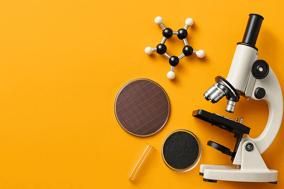
Adisyn Ltd (ASX:AI1) has announced a significant step forward in its quest to revolutionize semiconductor manufacturing with graphene interconnect technology. The company has successfully commissioned a new Beneq TFS 200 Atomic Layer Deposition (ALD) system at its R&D facility in Israel, replacing older legacy equipment. This upgrade marks the beginning of an intensive development phase aimed at overcoming the physical and performance limitations of copper interconnects in advanced semiconductor nodes below 5 nanometers.
Addressing a Critical Industry Bottleneck
As semiconductor chips shrink, copper interconnects; the tiny wiring that connects transistors; are hitting fundamental limits in speed, energy efficiency, and miniaturisation. Graphene, a single layer of carbon atoms arranged in a hexagonal lattice, offers exceptional electrical and thermal conductivity, making it a promising alternative. However, the industry has struggled to grow high-quality graphene directly on wafers at temperatures compatible with existing semiconductor processes.
Adisyn’s wholly owned subsidiary, 2D Generation, is pioneering a patented low-temperature ALD process using carbon-ring-based organic precursors. This approach enables direct graphene deposition at semiconductor-compatible temperatures, potentially unlocking a new generation of high-performance chips.
Phase One, Testing and Optimisation
The current phase focuses on precursor development and graphene growth optimisation. Using the new Beneq ALD system alongside parallel facilities at Tel Aviv University, Adisyn is conducting iterative test-refine cycles to evaluate multiple carbon-ring-based precursors. Key steps include plasma pre-cleaning to prepare substrates, controlled deposition sequences, post-deposition annealing to improve crystalline quality, and rigorous characterisation to feed back into the process.
This phase is expected to continue through 2025 and into early 2026, culminating in recipe development for uniformity, repeatability testing, wafer-scale integration, and industry collaboration for commercial trials.
A Globally Experienced Team and Strategic Partnerships
Adisyn’s development program is led by a multidisciplinary team of over 20 experts spanning Israel, Europe, and the US. Notable leaders include Chairman Kevin Crofton, a semiconductor industry veteran; Arye Kohavi, CEO of 2D Generation and renowned innovator; and VP R&D Miri Kish Dagan, an expert in semiconductor materials engineering.
The company also benefits from strategic partnerships with leading institutions such as Tel Aviv University’s Nano Center and imec, a global leader in nano and digital technologies. Additionally, Adisyn is part of the EU’s Connecting Chips program, collaborating with industry giants like NVIDIA and Applied Materials, although this program has yet to secure grant funding.
Looking Ahead
While still in early development, Adisyn’s low-temperature graphene ALD process holds promise to overcome a critical semiconductor bottleneck. The company plans to provide regular updates as it hits key technical milestones, potentially positioning itself at the forefront of next-generation chip manufacturing technology.
Bottom Line?
Adisyn’s graphene interconnect journey is gaining momentum, but the path to commercialisation remains a high-stakes race.
Questions in the middle?
- How will Adisyn’s graphene technology perform in wafer-scale integration and commercial trials?
- What impact will the pending EU Connecting Chips program funding have on development timelines?
- How does Adisyn’s approach compare with competing graphene interconnect technologies globally?