Adisyn Validates Key Step in Low-Temperature Graphene Process for Next-Gen Chips
Adisyn Ltd has successfully validated a critical pre-clean sub-process in its proprietary low-temperature graphene deposition method, marking a significant technical milestone toward revolutionizing semiconductor interconnects.
- Successful validation of wafer surface pre-clean sub-process
- Low-temperature graphene deposition process confirmed operational
- Advances aim to replace copper interconnects at sub-2nm nodes
- Next phase to focus on deposition trials and parameter optimization
- Global R&D collaborations underpin development progress

Technical Breakthrough in Graphene Deposition
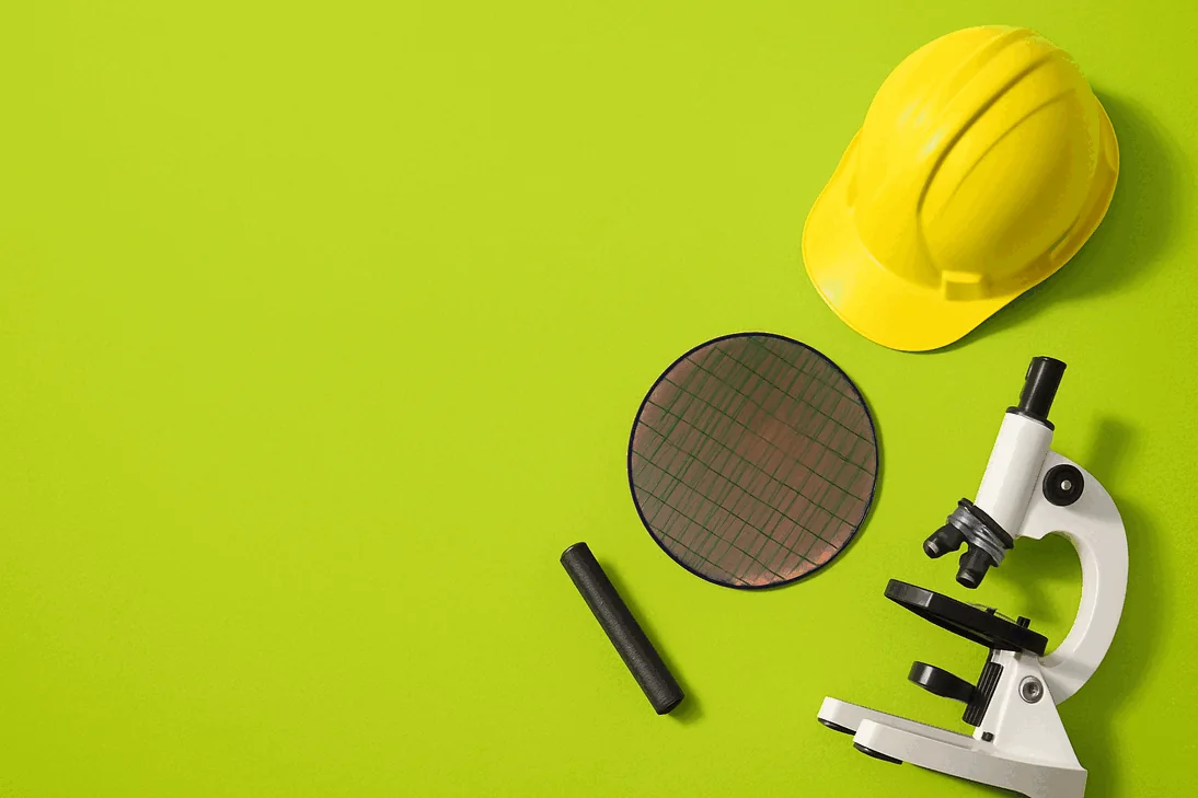
Adisyn Ltd (ASX:AI1) has announced a pivotal technical achievement in its graphene deposition development program, successfully validating a key sub-process within the wafer surface pre-clean stage. This step is essential for preparing semiconductor wafers to receive graphene films at low temperatures, a breakthrough that could redefine the future of chip manufacturing.
The company’s proprietary low-temperature Atomic Layer Deposition (ALD) technique targets one of the semiconductor industry's most pressing challenges, the physical and performance limits of copper interconnects as chip features shrink below 2 nanometers. Copper’s increasing electrical resistance and heat generation threaten the continued miniaturization and efficiency gains critical for advancing computing and AI technologies.
Why Graphene Matters
Graphene, a single-atom-thick layer of carbon atoms arranged in a hexagonal lattice, offers superior electrical conductivity, thermal resistance, and mechanical strength compared to copper. However, conventional graphene growth methods require temperatures exceeding 900°C, incompatible with standard semiconductor fabrication processes.
Adisyn’s low-temperature ALD process overcomes this barrier, enabling direct graphene growth on semiconductor wafers within industry-compatible temperature ranges. The successful validation of the pre-clean sub-process confirms that the company’s process architecture is functioning as designed, effectively preparing wafer surfaces for subsequent graphene deposition.
Next Steps and Industry Collaboration
Following this milestone, Adisyn will embark on extensive deposition trials using various carbon-ring-based precursor compounds. The company plans to refine remaining pre-clean sub-processes, optimize deposition parameters such as plasma power and gas flow, and thoroughly characterize the resulting graphene films for quality and conductivity.
These efforts are supported by a global, multidisciplinary R&D team spanning Israel, Europe, and the United States, with collaborations involving Tel Aviv University, imec in Belgium, and the EU Connecting Chips Initiative. This network positions Adisyn as a credible contender in the race to commercialize graphene for semiconductor interconnects.
Outlook
Adisyn remains on track to deliver progressive technical validations through late 2025 and into 2026, steadily advancing toward scalable graphene growth recipes. If successful, this technology could enable faster, smaller, and more energy-efficient chips powering the next generation of AI, computing, and communications devices.
Bottom Line?
Adisyn’s validated pre-clean step sets the stage for critical deposition trials that could transform semiconductor interconnect technology.
Questions in the middle?
- How will deposition trial results impact the timeline for commercial scalability?
- What competitive advantages does Adisyn’s low-temperature ALD process offer over other graphene growth methods?
- How might partnerships with global semiconductor leaders accelerate adoption?